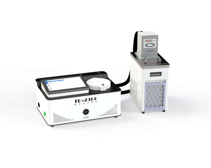


In modern chip manufacturing processes, specific surface area and true density are two extremely critical material characteristic parameters that run through every link from raw material quality control to chip performance optimization, playing a decisive role in the success or failure of chip manufacturing.
Specific surface area is an indicator of the size of a material's surface area per unit mass or volume, which directly reflects the surface activity and adsorption capacity of the material. In chip manufacturing, materials with high specific surface area can provide more active sites, which is beneficial for chemical reactions and substance adsorption. For example, in the preparation process of photoresist, a suitable specific surface area can ensure good adhesion between the photoresist and the substrate material, improving the accuracy and resolution of photolithography. In addition, the control of specific surface area during the modification and processing of chip surfaces directly affects the processing effect and the performance of the final product.
True density refers to the mass per unit volume of a material in a fully dense state, which reflects the density and uniformity of the internal structure of the material. In the production of semiconductor materials, precise true density testing can help producers detect impurities and defects in raw materials in a timely manner, ensuring that the silicon wafers put into production meet high-quality standards. In the process of chip packaging, the true density of packaging materials affects the stability and reliability of the packaging structure. Accurate true density data helps optimize packaging design, improve the product's ability to resist external interference, and extend its service life.
In the chip manufacturing process, precise detection and strict control of the specific surface area and true density of materials are key links to ensure chip performance, quality, and production efficiency, and have profound significance for promoting the sustainable development of the semiconductor industry.

contact
Be the first to know about our new product launches, latest blog posts and more.Any question or request?
Click below, we’ll be happy to assist. contact